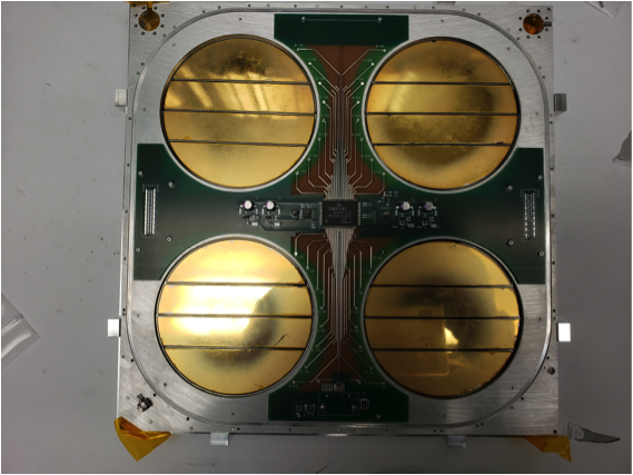
 Notional assembly of a GAPS "detector module". Visible are the four-strip Si(Li) detectors and some notional electronics. The flight version will use eight-strip Si(Li) detectors of similar overall dimensions. The connectors at the left and right sides of the board provide for power and signal passthrough. The bottom connector is for high voltage bias.
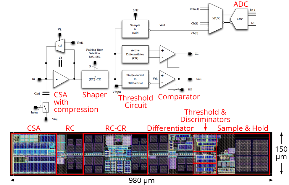 Block diagram (top) and layout (bottom) of a single GAPS electronics channel. The ADC and multiplexer layouts are not shown.
The 10-layer GAPS tracker is composed of 1,440 8-strip, 10-cm diamter, 2.5-mm thick lithium drifted silicon (Si(Li)) sensors instrumentng a 2.5-m3 volume. Seven planes are read out with custom application specific integrated circuits. The other three planes provide additional target mass and thermal balance. In order to achieve the target resolution of 4 keV FWHM at the X-ray energies, a custom readout system has been designed. The tracker electronics are required to generate high voltage for the detectors as well as low voltage rails, to readout the Si(Li) detectors with low noise, and to provide the interfaces necessary to transfer the information to the flight computer. The three sub-systems that constitute the tracker electronics are indicated, respectively, as power electronics, front-end electronics, and back-end electronics (or DAQ system).
The power electronics sub-system has the purpose of providing the bias voltage (HV) to the Si(Li) detector modules and the voltages (LV) to the front-end ASIC boards. The typical bias voltage of the Si(Li) detectors varies in the range 150-300 V, with a 1 V accuracy. The front-end electronics systems need four different bias voltages. The detectors are arranged in groups of four on what is called a "detector module". One detector module is instrumented by a single, 32-channels Application Specific Integrated Circuit (ASIC). We adopted a power distribution scheme where one LV channel provides voltage to a chain of six detector modules for an estimated power of 15 W. A custom power system able to manage the 360 HV channels (one per Si(Li) detector module) and the 60 LV channels (one per chain of six Si(Li) detector module) has been designed. The system has a microcontroller-based architecture and is interfaced with the GAPS DAQ system via Ethernet protocol.
The front-end electronics must handle a large range of signal amplitudes (20 keV - 50 MeV) and feature low noise performance in order to achieve the required 4 keV resolution at low energies. A custom 32-channel ASIC known as "Silicon LIthium DEtectors Readout" (SLIDER) has been developed for reading out the 11,520 Si(Li) strips of the GAPS silicon tracker. As already mentioned, the ASIC is located on a front-end board placed in the center of the Si(Li) detector module (Figure 1). The board distributes high voltage to the detectors, provides bias voltage and control signals to the ASIC, and propagates these signals throughout the whole tracker. Figure 2 shows the block diagram of one channel of the ASIC, and its layout. The analog signal processing scheme is based on a low-noise charge-sensitive amplifier (CSA) featuring dynamic signal compression. The solution takes advantage of the non-linear features of a MOS capacitor in the feedback loop of the charge-sensitive preamplifier itself. The amplifier is followed by a unipolar second order semi-Gaussian shaper. The signal peaking time at the shaper output is selectable among eight values (from 250 ns up to 2 µs). After the filtering stage, the analog signal is split into three different paths. On one side a comparator is used to recognize the presence of the amplified pulse. Another path includes a single-ended to differential sample-and-hold which stretches the signal peak and presents it to a successive approximation register (SAR) ADC for analog information detection. On the third path, the signal at the shaper output is differentiated. The identification of the zero-crossing of the resulting bipolar signal provides a trigger, synchronous with the shaper peaking time, to preset the single-ended to differential sample-and-hold.
The back-end electronics will configure, control and acquire data from the tracker front-end boards. A chain of six Si(Li) detectors modules (six ASICs) is controlled by one back-end channel through SPI protocol. One 6-channels FPGA-based DAQ box controls a tracker plane. The whole system comprises 10 DAQ boxes.